RISC V Pipelined Processor
In this blog post, we will explore the implementation of a pipelined RISC-V processor using Verilog, a hardware description language.


A pipelined processor is a symphony of synchronized stages
In this blog we'll be looking at the implementation of a 4-stage pipelined processor.
The processor supports:
- addition (add)
- shift left logical (sll)
- unconditional jump (j)
The processor implements forwarding to resolve data hazards.
Inputs
- Reset
- Clock
Outputs
None
Components
- Instruction Fetch Unit (IF)
- Register File (8 8-bit registers)
- Execution Unit (EX)
- Writeback Unit (WB)
Read and write operations on register file can happen simultaneously and should be independent of clock.
Pipelining
Pipelining is a technique used to enhance processor performance by overlapping instruction execution. It divides the processor's execution path into several stages, allowing multiple instructions to be processed simultaneously. Each stage performs a specific operation, such as instruction fetch, decode, execute and writeback. By breaking down the execution into smaller tasks, pipelining significantly improves the processor's throughput and performance.
Pipelined Registers
In order for pipelining to happen we need to store the results from the individual functional components at the end of every clock cycle so that it can be picked up in the next clock cycle by the next component in the pipeline. For this we'll be using pipeline registers.
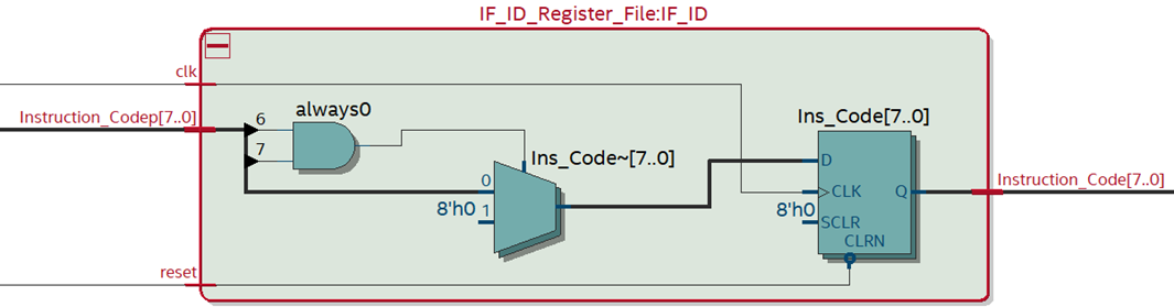
- IF/ID
- ID/EX
- EX/WB
When reset is activated, the program counter, pipelined registers are initialized to 0 and the instruction memory and register file get loaded by predefined values.
When the instruction unit starts fetching the first instruction, the pipeline registers contain unknown values.
When the second instruction is being fetching in the IF unit, the IF/ID registers will be hold the instruction code for the first instruction.
When the third instruction is being fetched by the IF unit, IF/ID register contains the instruction code of the second instruction and the ID/EX register contains information relevant to the first instruction and so on. This in summary is the essence of pipelining.
We will further assume an 8-bit program counter. The address and the data size is 8-bits as well.
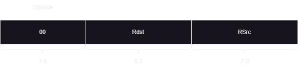
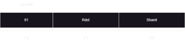
Instruction Classes
The first class of instructions would look something akin to below.
add R2, R0 (R2⬅️R2+R0)
The second class of instruction would look like below:
sll R0, 4 (R0⬅️R0<<4)
Finally the jump instruction would look like so:
j L1 (Jump address is calculated using pseudo direct addressing)

Processor Overview
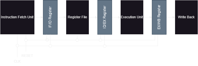
Overview of Final Design
Before delving into the gory details of every module, lets look at all the components and their connections in all their glory. We'll first look at a more simplified diagram and then look at something more detailed.
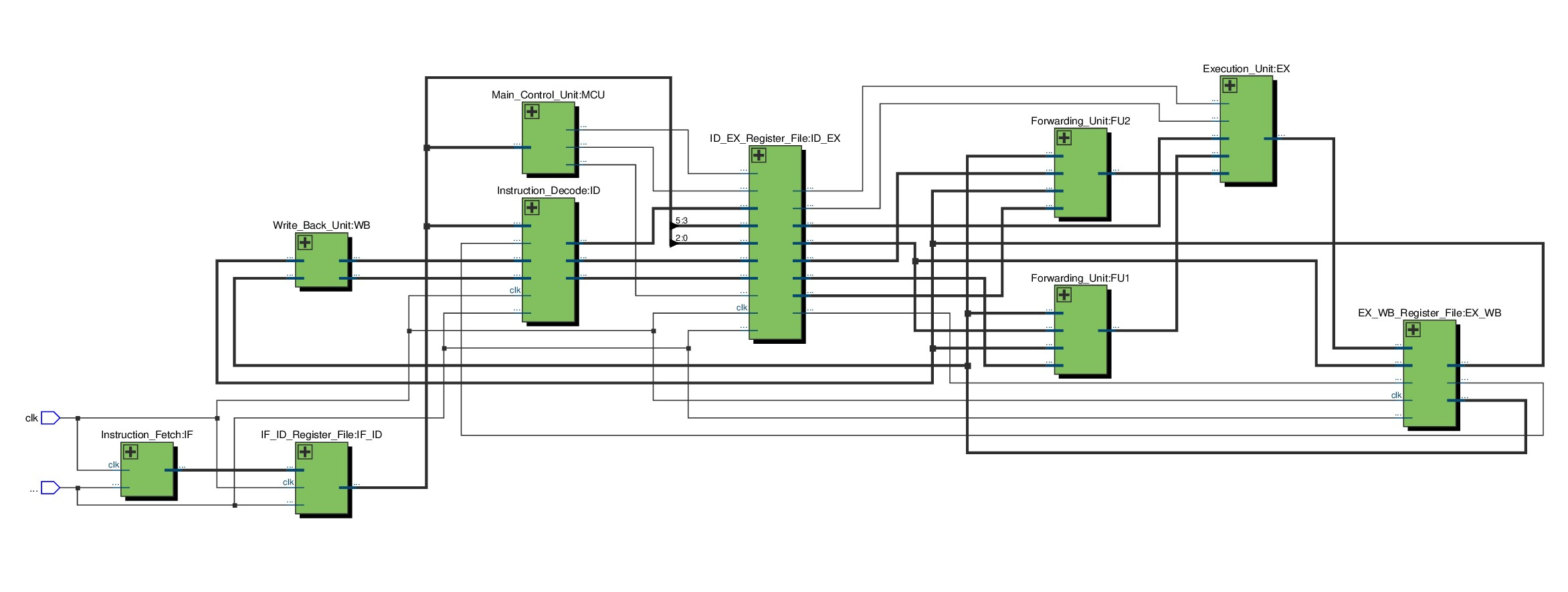
As we can see, the clock and reset inputs get fed to the instruction fetch, instruction decode and pipeline registers. A more detailed diagram is shown below:
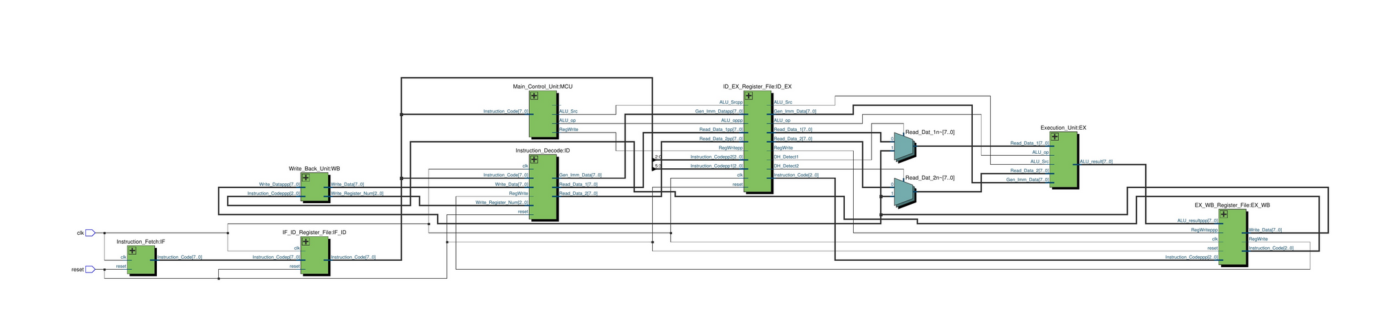
The blocks individually are as shown below:
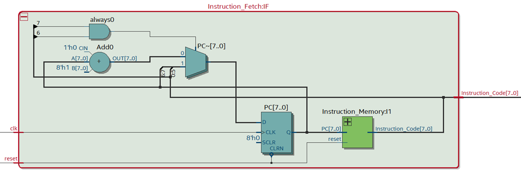
- Instruction Fetch Unit
The IF stage is responsible for fetching instructions from memory based on the program counter (PC) value. It retrieves the instruction from memory and passes it to the next stage, the Instruction Decode (ID) stage. In Verilog, this stage involves reading the instruction memory and updating the program counter accordingly.
2. IF/ID Register File:
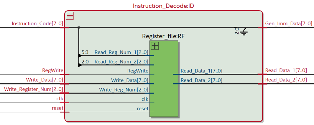
3. Instruction Decode Unit:
In the ID stage, the fetched instruction is decoded to determine the operation to
be performed. It involves extracting the opcode and operands from the
instruction and fetching the corresponding values from the register file.
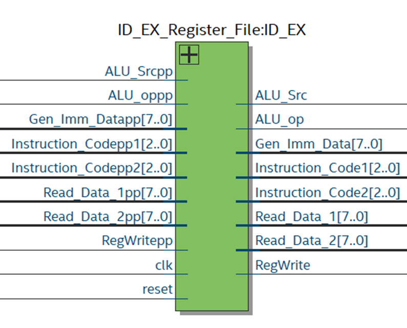
4. ID/EX Register File
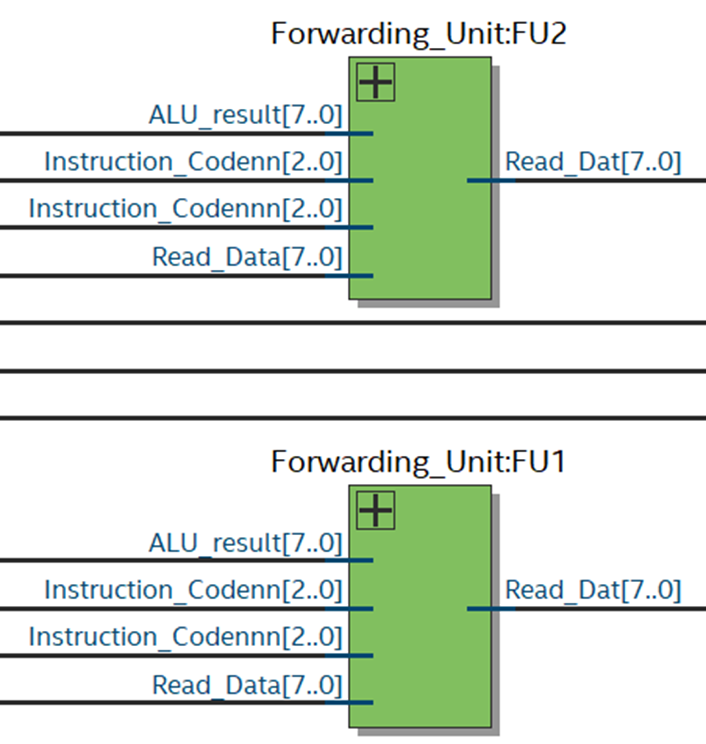
5. Forwarding Units
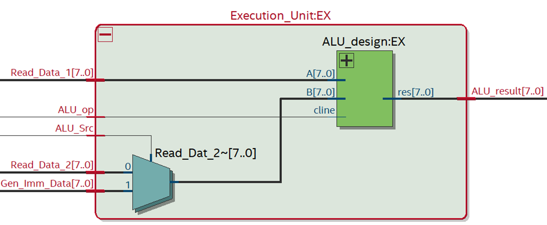
6. Execution Unit
The EX stage executes the arithmetic and logical operations specified by the
instruction. It performs calculations, such as addition and logical operations, on
the operands obtained from the ID stage. The ALU (Arithmetic Logic Unit) is a
critical component of this stage.
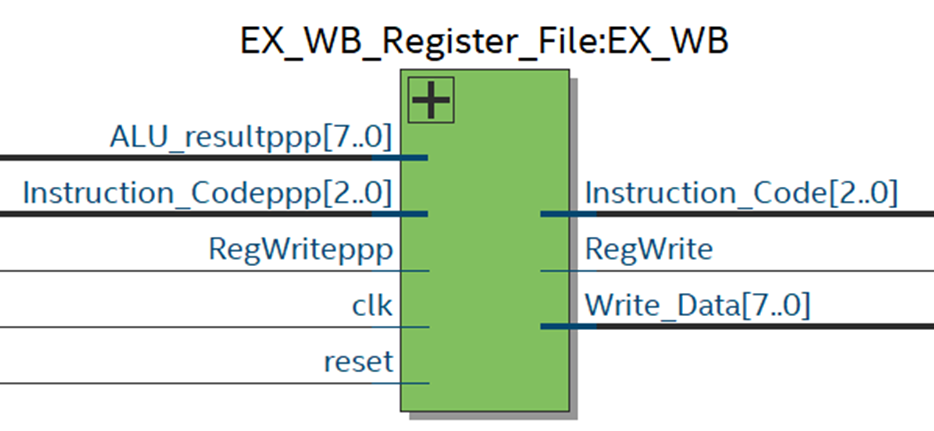
7. EX/WB Register File
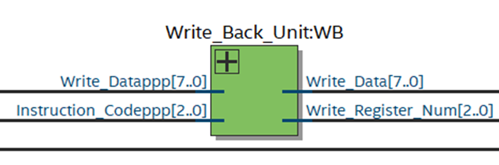
8. Write Back Unit
The final stage, WB, is responsible for writing the result back to the register file.
It receives the data from the previous stage and updates the destination register
with the computed value. This stage ensures that the final result is correctly
stored for future instructions or output.
Control Signals
|
Instructions |
Control
Signals |
||
|
|
|
|
|
|
add |
|
|
|
|
sll |
|
|
|
|
j |
|
|
|
Data Hazards
Data Hazards can be detected when
- The destination register in the EX/WB Pipeline Register and ID/EX Pipeline Register is the same
OR - The destination register in the EX/WB Pipeline Register and the source register in the ID/EX Pipeline Register is the same.
Conclusion
Implementing a pipelined RISC-V processor in Verilog provides a deeper understanding of processor architecture and the intricacies of instruction execution. By breaking down the execution into separate stages and leveraging Verilog's power, we can design a high-performance processor capable of executing complex tasks efficiently.
All the code for this processor architecture can be found here