RISC V Single Cycle Processor

In the world of computer architecture, the single-cycle processor is a testament to simplicity and efficiency.
We'll be looking at the datapath and the control unit for a single cycle processor with two classes of instructions
Immediate Type
Example li, r1, constant ➡️loads immediate signed value specified in the instruction to the register R1

Register Type (R-type)
Example: add r1, r2, r3 ➡️adds contents of registers r2 and r3. The result of addition is written to register r1

Further we'll assume that there are 32 32-bit general purpose registers indicated by r0, r1, r2.....r31 and corresponding register numbers (00000), (00001)......(11111).
The Opcode for Immediate type and R-type instructions are as below:
|
Instruction Class |
Opcode |
|
Immediate type |
111111 |
|
Register Type |
000000 |
Additionally R-type instructions have multiple variations defined by their function codes. The R-type instructions include add, sub, AND, OR, srl (Shift right logical), sll (shift left logical). The different R-type instructions that the processor supports are tabulated below:
|
R-type Instruction |
Example usage |
Opcode |
Rdst |
Rsrc1 |
Rsrc2 |
shamt |
Function |
|
add |
add r0, r1, r2 |
000000 |
00000 |
00001 |
00010 |
00000 |
100000 |
|
sub |
sub r4, r5, r6 |
000000 |
00100 |
00101 |
00110 |
00000 |
100010 |
|
AND |
and r8, r9, r10 |
000000 |
01000 |
01001 |
01010 |
00000 |
100100 |
|
OR |
and r9, r8, r10 |
000000 |
01001 |
01000 |
01010 |
00000 |
100101 |
|
sll |
sll r11, r6, 6 |
000000 |
01011 |
00110 |
00000* |
00110 |
000000 |
|
srl |
srl r13, r9, 10 |
000000 |
01101 |
01001 |
00000* |
01010 |
000010 |
The processor module has only two inputs CLK and Reset. When Reset is activated the Processor starts executing instructions from 0thlocation of instruction memory.
Implementation
The overall block diagram is as shown:

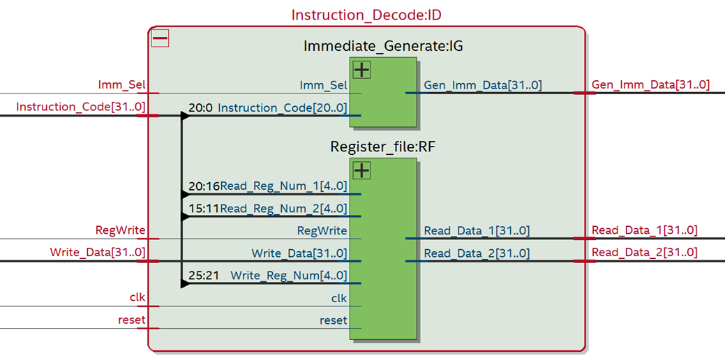
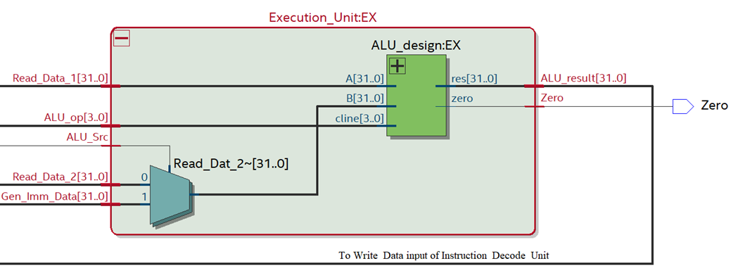
At a high level, there are 4 primary units that comprise the system:
- Instruction Fetch Unit that includes the instruction memory and the processor clock

2. Main Control Unit

3. Instruction Decode Unit which includes the register file and the immediate generate segment

4. Execution Unit which includes the ALU and the ALU Source multiplexer

All the code for this implementation can be found here

